Data Sheet
V 1.0 / May. 2017
MSM261D4020H1AP
PDM digital output MEMS microphone with Multi‐modes
© 2
MSM261D4020H1AP
PDM digital output MEMS microphone
GENERAL DESCRIPTION
MSM261D4020H1AP is an
omnidirectional, Top‐ported, PDM digital
output MEMS microphone. It has high
performance and reliability.
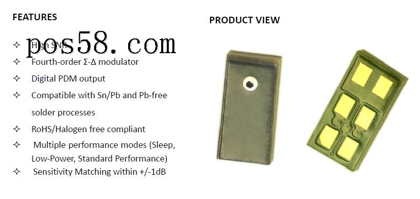
MSM261D4020H1AP is available in a thin
4 mm × 2 mm × 1 mm proprietary OCLGA
package. It is SMT compatible with no
sensitivity degradation.
FEATURES
High SNR
Fourth‐order Σ‐Δ modulator
Digital PDM output
Compatible with Sn/Pb and Pb‐free
solder processes
RoHS/Halogen free compliant
Multiple performance modes (Sleep,
Low‐Power, Standard Performance)
Sensitivity Matching within +/‐1dB
APPLICATIONS
Mobile Phone
Laptop
Tablet computer
Bluetooth headset
Earphone
Wearable intelligent equipment
PRODUCT VIEW
© 3
MSM261D4020H1AP
PDM digital output MEMS microphone
ABSOLUTE MAXIMUM RATINGS
Parameter Maximum value Unit
Supply Voltage −0.3 to 4.0 V
Sound Pressure Level 140 dB SPL
Temperature Range −40 to 100 °C
Electrostatic discharge protection 2 (HBM) kV
ACOUSTIC & ELECTRICAL SPECIFICATIONS
TEST CONDITIONS: 23 ±2°C, 55±20% R.H., VDD=1.8 V, fCLOCK=2.4 MHz, SELECT pin grounded, no
load, unless otherwise indicate
General Microphone Specifications
Parameter Symbol Conditions Min Typ Max Units
Supply Voltage VDD 1.6 ‐ 3.6 V
Clock
Frequency
Range
Sleep Mode 0 50 KHz
Low‐Power Mode 150 900 KHz
Standard Performance
Mode
1.1 4.0 MHz
Sleep Current ISLEEP fCLOCK ≤ 50 kHz ‐ 1 μA
DC Output Fullscale = ±100 ‐ 4 ‐ % FS
Directivity Omnidirectional
Polarity Increasing sound increasing density of 1’s
Data Format ½ Cycle PDM
Short Circuit Current ISC
Grounded DATA
pin
1
‐
10 mA
Output Load CLOAD ‐ ‐ 200 pF
Fall‐asleep Time fCLOCK ≤ 50 kHz ‐ ‐ 30 μs
Wake‐up Time fCLOCK ≥ 151 kHz ‐ ‐ 200 μs
Power‐up Time VDD ≥ V(min) ‐ ‐
50 ms
Mode‐Change Time ‐ ‐ 10 ms
© 4
MSM261D4020H1AP
PDM digital output MEMS microphone
Standard Performance Mode
TEST CONDITIONS: fCLOCK = 2.4 MHz, VDD=1.8 V, unless otherwise indicated
Parameter Symbol Conditions
Mi
n
Typ Max Units
Supply Current IDD fCLOCK=2.4 MHz ‐ 670 ‐ μA
Sensitivity S 94 dB SPL @ 1 kHz ‐27 ‐26 ‐25 dBFS
Signal to Noise Ratio SNR
20 kHz bandwidth, A‐weighted
fCLOCK=2.4 MHz
‐ 64 ‐ dB(A)
Total Harmonic
Distortion
THD 94 dB SPL @ 1 kHz, S = Typ ‐ 0.2 ‐ %
Acoustic Overload
Point
AOP 10% THD @ 1 kHz, S = Typ ‐ 120 ‐ dB SPL
Power Supply
Rejection Ratio
PSRR 200 mVpp sinewave @ 1 kHz ‐ 50 ‐ dBV/FS
Power Supply
Rejection
PSR+N
100 mVpp square wave @ 217 Hz,
A‐weighted
‐ ‐80 ‐ dBFS(A)
© 5
MSM261D4020H1AP
PDM digital output MEMS microphone
Low‐Power Mode
TEST CONDITIONS: fCLOCK =768 kHz, VDD=1.8 V, unless otherwise indicated
Parameter Symbol Conditions Min Typ Max Units
Supply Current IDD fCLOCK=768KHz ‐ 290 ‐ μA
Sensitivity S 94 dB SPL @ 1 kHz ‐26 ‐25 ‐24 dBFS
Signal to Noise
Ratio
SNR
94 dB SPL @ 1 kHz,
A‐weighted(20Hz‐8KHz)
‐ 62 ‐ dB(A)
Total Harmonic
Distortion
THD 94 dB SPL @ 1 kHz, S = Typ ‐ 0.2 ‐ %
Acoustic Overload
Point
AOP 10% THD @ 1 kHz, S = Typ ‐ 120 ‐ dB SPL
Power Supply
Rejection Ratio
PSRR 200 mVpp sinewave @ 1 kHz ‐ 50 ‐ dBV/FS
Power Supply
Rejection
PSR+N
100 mVpp square wave @ 217 Hz,
A‐weighted(20Hz‐8KHz)
‐ ‐80 ‐ dBFS(A)
Microphone Interface Specifications
Parameter Symbol Conditions Min Typ Max Units
Logic Input High VIH 0.7xVDD ‐ 3.6 V
Logic Input Low VIL ‐0.3 ‐ 0.3xVDD V
Logic Output High VOH IOUT = 2 mA VDD ‐0.45 ‐ ‐ V
Logic Output Low VOL IOUT = 2 mA ‐ ‐ 0.45 V
Clock Duty Cycle ‐ 40 ‐ 60 %
© 6
MSM261D4020H1AP
PDM digital output MEMS microphone
MICROPHONE STATE DIAGRAM
Standard Performance Mode
3.6 ≥ VDD ≥ 1.6 V
1.1 MHz ≤ fCLOCK ≤ 4MHz
Powered Down
Mode
VDD = 0 V
Sleep Mode
3.6 ≥ VDD ≥ 1.6 V
fCLOCK ≤ 50 kHz
Low‐Power Mode
3.6 ≥ VDD ≥ 1.6 V
150 kHz ≤ fCLOCK ≤ 900 kHz
© 7
MSM261D4020H1AP
PDM digital output MEMS microphone
TYPICAL FREQUENCY RESPONSE
‐20
‐10
0
10
20
Sensitivity (dB FS/Pa)
Frequence (Hz)
Frequency Response @94dB SPL
100 200 500 1K 2K 5K 10K
TIMING DIAGRAM
Parameter Symbol Min Typ Max
Clock Rise/Fall Time tEDGE ‐ ‐ 13ns
Delay Time to High Z tDZ 3ns ‐ 16ns
Delay Time to Data Line Driven tDD 18ns 28ns 40ns
※ tHOLD and tDV are related to load.
© 8
MSM261D4020H1AP
PDM digital output MEMS microphone
SMT Parameters:
1. Recommend PCB land pattern layout:(unit: mm)
© 9
MSM261D4020H1AP
PDM digital output MEMS microphone
2. Recommend reflow profile:
Description Parameter Pb‐free
Average ramp rate TL to TP 3 °C/sec max
Preheat
Minimum temperature
Maximum temperature
Time(TSMIN to TSMAX)
TSMIN
TSMAX
tS
150 °C
200 °C
60 sec to 120 sec
Ramp‐up rate TSMAX to TL 1.25 °C/sec max
Time maintained above liquidus temperature
Liquidus temperature
tL
TL
60 sec to 150 sec
217 °C
Peak temperature TP 260 °C max
Time within 5°C of actual peak temperature tP 20 sec to 40 sec
Ramp‐down rate TL to TP 6 °C/sec max
Time 25 °C (t25 °C) to peak temperature t 8 minutes max
© 10
MSM261D4020H1AP
PDM digital output MEMS microphone
OUTLINE DIMENSIONS AND PIN DEFINITION:
PIN function description
PIN# Function
1 VDD
2 DATA
3,4 GND
5 CLK
6 L/R
Item Dimension Tolerance
Length (L) 4.00 ±0.10
Width (W) 2.00 ±0.10
Height (H) 1.00 ±0.10
Port (AP) Ø0.325 ±0.05
Dimensions are in millimeters
Tolerance is ±0.15mm unless otherwise specified.
TOP VIEW SIDE VIEW BOTTOM VIEW
© 11
MSM261D4020H1AP
PDM digital output MEMS microphone
ADDITIONAL NOTES
(A) MSL (moisture sensitivity level) Class 2a.
(B) Maximum of 3 reflow cycles is recommended.
(C) In order to minimize device damage:
Do not board wash or clean after the reflow process.
Do not brush board with or without solvents after the reflow process.
Do not directly expose to ultrasonic processing, welding, or cleaning.
Do not insert any object in port hole of device at any time.
Do not apply air pressure into the port hole.
Do not pull a vacuum over port hole of the microphone.
MATERIALS STATEMENT
Meets the requirements of the European RoHS and Halogen‐Free.
© 12
MSM261D4020H1AP
PDM digital output MEMS microphone
PACKAGING & MARKING DETAIL:
Note:
1) Dimensions are in mm;
2) Don't put the vacuum suction nozzle alignment the port hole;
3) Tape &Reel Per EIA‐481 standard;
4) Label applied to external package and direct to reel;
5) Static voltage <100V;
Model Number Reel Diameter Quantity Per Reel
MSM261D4020H1AP 13 inch 5700
© 13
MSM261D4020H1AP
PDM digital output MEMS microphone
RECOMMENDED INTERFACE CIRCUIT:
Figuer 1. MSM261D4020H1AP electrical connections
LR
MIC
10uF
100nF
VDD
LR DATA
CLK
CODEC
GND VDD
Figuer 2. Electrical connections for stereo configurations
GND
LR DATA
VDD
CODEC
VDD
MIC1 MIC2
VDD
CLK
GND
LR DATA
VDD
CLK
10uF
100nF
Power supply decoupling capacitors (100nF ceramic,10uF ceramic) should be placed
as near as possible to VDD of the device.(common design practice)
© 14
MSM261D4020H1AP
PDM digital output MEMS microphone
RELIABILITY SPECIFICATIONS
NOTE: Sensitivity should vary within ±3dB from initial sensitivity. (The measurement to be
done after 2 hours of conditioning at 20±2℃, R.H 60%~70%)
Test Description
Thermal Shock
100 cycles air‐to‐air thermal shock from ‐40oC to +125oC with 15
minute soaks. (IEC 68‐2‐4)
High Temperature
Storage
1,000 hours at +105oC environment (IEC 68‐2‐2 Test Ba)
Low Temperature Storage
1,000 hours at ‐40oC environment (IEC 68‐2‐2 Test Aa)
Reflow 5 reflow cycles with peak temperature of +260oC
ESD‐HBM/LID‐GND
3 discharges of ±2 kV direct contact to I/O pins. (MIL 883E, Method
3015.7)& 3 discharges of ±8 kV direct contact to lid while unit is
grounded. (IEC 61000‐4‐2)
Vibration
4 cycles of 20 to 2,000 Hz sinusoidal sweep with 20 G peak
acceleration lasting 12 minutes in X, Y and Z directions. (Mil‐Std‐883E,
Method 2007.2 A)
Mechanical Shock
3 pulses of 3,000 G in the X, Y and Z direction (IEC 68‐2‐27, Test Ea)
High Temperature Bias
1,000 hours at +105oC under bias (IEC 68‐2‐2 Test Ba)
Low Temperature Bias
1,000 hours at ‐40oC under bias (IEC 68‐2‐2 Test Aa)
Temperature/Humidity
Bias
1,000 hours at +85oC/85% R.H. under bias. (JESD22‐A101A‐B)
Drop Test
To be no interference in operation after dropped to 1.0cm steel plate
18 times from 1.5 meter height
© 15
MSM261D4020H1AP
PDM digital output MEMS microphone
REVISION HISTORY:
Revision Subjects (major changes since last revision) Date
0.8 Preliminary Edition 2017‐02‐22
1.0 Initial Release 2017‐05‐05 |